
This is a sub-section of my posts describing the Sustainable Energy Design 3 course group project to Design and Build a Micro Wind Turbine – for more information see here
So that you can manage calculations for the divider you need to know the value of the input voltage and to do this you need a voltage regulator. There two types of these:
- linear voltage supply – always creates a loss in voltage because of its design
- switched power supply – can be buck, boost, or buck-boost converters.
Designing the generator specification had been done early on in the project because the deadline for ordering components in time was very early on in the project. However this had resulted in designing in something of a hurry and in that I had made a very large mistake – I hadn’t accounted for the voltage losses across the rectifier circuit. Although the generator itself would be producing sufficient voltage, once converted to DC the rectifier output was theoretically only about about 9V.
Therefore the voltage regulator could be used as an opportunity to compensate somewhat for this by using a boost DC-DC converter to amplify the voltage to at least the minimum required voltage for charging.
We needed a boost converter that used a through hole mounting type so it can be used with the breadboard prototype, and convert an input voltage of 9V to an output voltage of at least 14V, and a quick search found the LT1303 model to be a reasonable choice. Figure 1 shows a typical use of the LT1303 below.
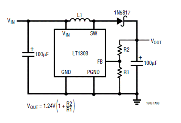
Instead of using a 1N5817 diode in the example usage we can use another one of our Schottky diodes from the rectifier.
The voltage regulator inductors:
- typically in the 5mH to 50mH rangefor this kind of application
- need to handle 1.25A current without saturating
- need to have enough inductance to provide a di/dt lower than 400mA/ms
- need to have low enough resistance to avoid heating losses
I chose to use a 10mH radial ELC18B inductor as it complied with all the above specifications. Although higher values inductors are better for the higher power, they are considerably larger in physical size and thus reducing practicality of the product, and are increasingly more expensive, unjustifiably so for our limited budget.

The Potentiometer
As part of the circuit for the voltage regulator in the Battery Management System circuit design, a potentiometer is necessary to vary resistance. The microcontroller has digital outputs and can approximate an analogue one with pulsed width modulation (PWM) allowing for either digital or analogue control. This gives three main options for varying the resistance:
- Digital potentiometer
- Multiplying Digital to Analogue converter
- Build a custom circuit
Digital Potentiometers
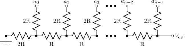
These are normally resistance ladders like Figure 3 below, they are the cheapest option and are widely used.
The main disadvantages are that they are constrained by current limit in the range of tens of milliamperes and most digital potentiometers limit the input voltage range to the digital supply range of 0–5 VDC. Additionally, they have discrete steps in resistance as opposed to the continuous (or at least approximately) variation achievable by other circuits. Also they generally have very poor tolerances of around 20% and poor temperature coefficients which could significantly affect the accuracy of the circuit. However, this could potentially be accounted for in the Kalman filter code (see the State of Charge use of Kalman Filters for more information).
Every step on the resistor ladder has its own switch which can connect this step to the output terminal of the potentiometer. The selected step on the ladder determines the resistance ratio of the digital potentiometer. The number of steps is normally indicated with a bit value e.g. 8 bits equals 256 steps; 8 bits is the most common, but resolutions between 5 and 10 bits (32 to 1024 steps) are available.
Multiplying Digital to Analogue Converter (DAC)
There are several DAC architectures multiplying DAC used as a digital potentiometer Typically a signal span of +15V to -15V is possible, with 16 bit control, i.e. 65535 discrete set points, and drift and non-linearity are negligible. However a DAC has to be initialised each time it switches on although this can be done through the microcontroller. A multiplying DAC cannot be directly used as a rheostat which could limit some design options.
Final Design
Although not ideal, because of costing we chose a digital potentiometer as opposed to a more generalised DAC. We wanted one that is through hole mounted (so it can easily be used in the breadboard prototype) and communicates via a protocol that the microcontroller preferably has a library to interface with such as I2C or SPI. So we chose the Microchip MCP41100 that uses SPI, a setting time of 18μs (with +- 1% error band), and has 256 linear taps which means it can be adjusted across 256 different linear values (defined in hex through SPI protocol).
It has a shutdown feature that disconnects the “A” terminal from the resistor stack and simultaneously connects the wiper to the other terminal so the values in the wiper register can be changed and it returns from shutdown to the new value. This can either be triggered through hardware with the shutdown pin, or internally through software control. For the purpose of our application, I tied the shutdown higher in the hardware as I do not feel it necessary to use but this allows for potential future design improvements as it could be used to implement an emergency shutdown procedure in case of the microcontroller identifying the battery significantly overcharging.
Code 00h effectively connects the wiper to the B terminal. At power-up, all data registers will automatically be loaded with the mid-scale value (80h). The serial interface provides the means for loading data into the shift register, which is then transferred to the data registers.
The ideal Vdd (value to power the IC itself, not the input to the potentiometer) is 5V, absolute maximum 7V, and so we have connected it to the same power supply as the microcontroller at around 3V3 which although not ideal, is still within the safe limits. This is because the datasheet specifies that all inputs and outputs with respect to VSS must be between 0.6V and VDD +1.0V, so if the digital control inputs from the microcontroller are to work they need to be within that range and this is more easily defined if Vdd is simply the same for both.
The datasheet also recommends using bypass capacitors, placed as close as possible to the device pin, and so one of 0.1 μF has been used in the charging circuit. It also recommends that the digital and analogue paths “should be separated as much as possible on the board, with no traces running underneath the device or the bypass capacitor”. This is of course most important with the clock line because of its high frequency. This is difficult to implement on the breadboard prototype due to the limited space, however is a factor in the PCB design.

From the datasheet we are provided with Figure 5 from which we can see the equation from which we can calculate the resulting resistance implemented from different input values of Dn. This is what is implemented into the code to adjust the different inputs to the battery.
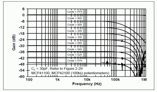
We can also see in Figure 6 the effect on gain of different values or codes input and the relationship with frequency as this is a feature to be aware of in designing the circuit, although for our ideal values, this suggests no immediate problems.
Next: The Complete Circuit Design
This is a sub-section of my posts describing the Sustainable Energy Design 3 course group project to Design and Build a Micro Wind Turbine – for more information see here
