
This is a sub-section of my posts describing the Sustainable Energy Design 3 course group project to Design and Build a Micro Wind Turbine – for more information see here
Final Circuit Design

Manufacturing Charging Circuit
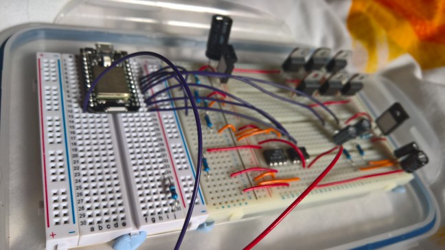
Breadboards are only designed for microelectronics prototyping and not typically for power electronics, and so although we are only handling relatively low voltages, currents and power from the generator, it isn’t suitable for final implementation. Ideally breadboards should only have around 1A going through them and so our ideal expected generator output of 5A could in the worst case damage the board and components, in the optimal case just create significant losses. However because it is flexible it is suitable for prototyping circuits to test individual features (see Appendices for more information).
To manufacture the final PCB circuit we are using the university’s in house etching facilities in the electronics laboratories as this is both quicker and cheaper than using external services to do this. This does have the disadvantage that the university cannot create any “through-hole-plating”, which is required to make automatically connections from the top of the board to the bottom but for our circuit this shouldn’t be too problematic. Additionally there is no solder-resist and no screen-print (labelling printed on the board) but these are not significant issues.
To use this facility the circuit needs to be modelled in Target 3001! CAD software and the files sent to be printed onto a special semi-transparent film with an ink-jet printer. Then, using a photographic process this is transferred to a special orange film to improve the quality of the PCB. The PCB itself comes from the suppliers coated with a photo-sensitive film that shields the copper from the etching agent chemical once it has been developed, and the holes are drilled into the board with a special drill. The black plastic can then be removed, the orange film aligned with the holes and the whole thing exposed to UV light. The pattern is now on the PCB which is then developed so the copper no longer needed is actually exposed, and then etched away in a tank of ferric-chloride. Unfortunately due to health and safety regulations we are unable to carry out this process ourselves and must be done by staff.
We could potentially laser cut the copper paths ourselves but this generally requires a very accurate laser cutter which we do not affordably have access to, and is a process known to commonly create accidental short cuts in the circuit. Using a larger machine to mill or drill it out provides difficulties with vibrations and holding the PCB board in place during manufacturing, as this would ideally be done with a vacuum facility that also we do not have.
Next: And The Rest Of It…
This is a sub-section of my posts describing the Sustainable Energy Design 3 course group project to Design and Build a Micro Wind Turbine – for more information see here
